Home
FPGA + PCIe Hardware Accelerator Design Walkthrough (DDR3, M.2, ..) - Phil's Lab #82
Phil’s Lab
Nov 4, 2022
162,040 views
Differential Pairs - PCB Design Basics - Phil's Lab #83
2-Layer PCB Design Tips - Phil's Lab #137
How To Do Ethernet in FPGA - Easy Tutorial
BGA PCB Design Tips - Phil's Lab #95
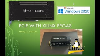
PCIe on Xilinx FPGAs
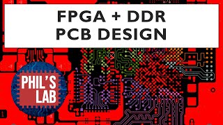
FPGA/SoC + DDR PCB Design Tips - Phil's Lab #59
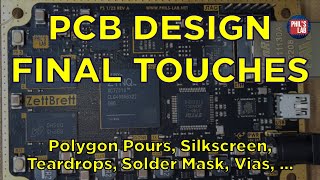
PCB Design Final Touches (Tips & Checklist) - Phil's Lab #131
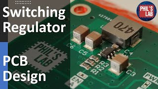
Switching Regulator PCB Design - Phil's Lab #60
No, Einstein Didn’t Solve the Biggest Problem in Physics
Tesla's Self-Driving Is Going Global
How To Create Difficult FPGA Designs with CPU, MCU, PCIE, ... ( with Adam Taylor )
KiCad 6 STM32 PCB Design Full Tutorial - Phil's Lab #65
ESP32 + PCB Antenna Hardware Design Tutorial - Phil's Lab #90
Mini 6-Layer Mixed-Signal Hardware Design Walkthrough - Phil's Lab #78
M.2 System-on-Module Hardware Design - Phil's Lab #107
How To Learn PCB Design (My Thoughts, Journey, and Resources) - Phil's Lab #87
KiCad 7 STM32 Bluetooth Hardware Design (2/2 PCB) - Phil's Lab #128
Extracting Firmware from Embedded Devices (SPI NOR Flash) ⚡
KiCad 7 STM32 Bluetooth Hardware Design (1/2 Schematic) - Phil's Lab #127