Home
IEDM tutorial: Beyond FINFET era Challenges and opportunities for CMOS technology
Science and Technology
May 27, 2022
2,771 views
The Gate-All-Around Transistor is Coming
Bob Patti: Advanced Packaging of Semiconductors
Nanoscale FinFET Technology for Circuit Designers, by Dr. Alvin Loke - Nov. 2021.
Innovations in AI Chip Packaging: Advanced Processes & Equipment Technologies
Webinar 4 | Semiconductor Processes: From Bare Wafer to Test
The A to Z of Multi-Die Design: Stage Chiplets Building the Future of SoCs
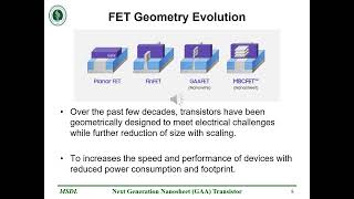
Next Generation Nanosheet GAA Transistor
Advanced Packaging for Heterogeneous Integration
What is wrong with 5nm, 3nm, 1nm.. CPU Technology Nodes explained
VLSI- Photonics-electronics Convergence Technology to Accelerate Innovative Optical Wireless Network
The Challenges for Organic or Glass Core Substrates as Advanced Packaging RDL at 2 µm L/S and Beyond
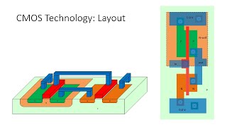
CMOS Tech: NMOS and PMOS Transistors in CMOS Inverter (3-D View)
GLOBALFOUNDRIES Webinar: Extending Moore's Law with FD-SOI Technology
FinFET Design By Dr K G Sharma
Stacking Dies For Performance and Profit
Heterogeneous IGZO Si CFET Monolithic 3D Integration
QCW CO2 Laser Drilling for Flip chip ball grid array (FCBGA) Applications
L2-A The Future of Moore's Law: What will be used in 3nm, 2nm, 1nm nodes?
Next-Gen Transistors
FinFETs