Home
Tackling Advanced Analog FinFET Back-end Layout
Cadence Design Systems
3 ส.ค. 2023
การดู 1,616 ครั้ง
Nanoscale FinFET Technology for Circuit Designers, by Dr. Alvin Loke - Nov. 2021.
Crossing the Chasm
Future Computers Will Be Radically Different (Analog Computing)
CEDA Distinguished Speaker at DATE 2023: Jan M. Rabaey
Do not be afraid of UVM
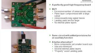
High Speed and RF Design Considerations
Advanced Process Technologies - Part 2: Fabricating a FinFET
Mood Booster 🌻Best Songs You Will Feel Happy and Positive After Listening To It (Immediate Effect)
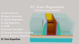
FinFET process flow
ISSCC2020: Plenary - Future Scaling: Where Systems and Technology Meet
สอนวิธีเขียน Prompt ที่ดี ให้ ChatGPT ช่วยคุณทำงานได้จริง!
L10B - Cadence Generic 14nm FinFET Layout and Structure (Part I)
Figma for Education: Learning Auto layout
Introduction to FinFETs
12 반도체 패키징 Advanced Packaging 2.5D, 3D -인하대 주승환교수
เลิกใช้ External HDD เลิกใช้ Google Drive แล้วจะใช้อะไรแทน?
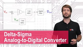
Analog-to-Digital Converters (ADC) - Charge-Balancing and Delta-Sigma ADC
Differential Pair Analog Layout and Matching Techniques in Cadence Virtuoso in 45nm CMOS | Part-1
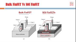
FinFET Structures
Tech CEO: แชร์วิธีการทำงานของ AI