Home
SR Latch Timing Diagram or waveform , Characteristic Equation
GATE CSE LECTURES BY AMIT KHURANA
Nov 22, 2022
3,988 views
Introduction to D Latch | Circuit, Working, Truth Table, Characteristic Equation & Excitation Table
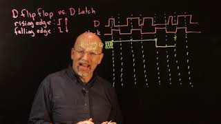
Ep 058: Timing Diagrams of Flip-Flops and Latches
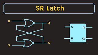
SR latch
8 - All About Flip-Flops: SR Flip-Flop, JK Flip-Flops, D Flip-Flops, T Flip-Flop Explained
How to draw timing diagram for D Latch and D Flip-flop?
Gated SR latch | SR Latch
SR Latch Circuit - Basic Introduction
Latches and Flip-Flops 2 - The Gated SR Latch
Preset & Clear Inputs in Flip flop | Asynchronous Inputs
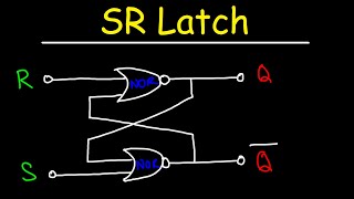
SR Latch | NOR and NAND SR Latch
Gated SR Latch | SR Latch with Enable or Control Input | Timing Diagram of Gated SR Latch
SR Latch and Gated SR Latch Explained | SR Latch using NOR gates and NAND gates
JK Flip Flop | Part 1
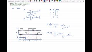
SR Latch Timing Diagram
Concept of Triggering | Level Trigger vs Edge Trigger Flip Flop
LEC 8: Timing Diagram Of SR Flip Flop
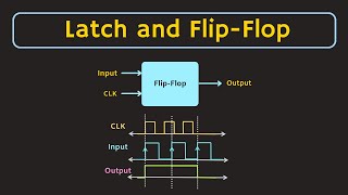
Latch and Flip-Flop Explained | Difference between the Latch and Flip-Flop
Timing Diagram of SR Latch: Sequential Circuits in Digital Logic Design
SR Flip-Flop using NOR gate || SR Flip-Flop || RS Flip-Flop using NOR gate || RS Flip-Flop || STLD |