Home
FinFET Technology (Basics, Structure, Characteristics, Merits, Demerits & Applications) Explained
Engineering Funda
Mar 3, 2021
58,409 views
OR Gate in Xilinx using Verilog/VHDL | VLSI by Engineering Funda
MOS Transistor (Basics, Types, Structure & Working of n channel MOSFET) Explained
FinFET Technologies for Analog Design
The Gate-All-Around Transistor is Coming
7nm FINFET Layout
What is wrong with 5nm, 3nm, 1nm.. CPU Technology Nodes explained
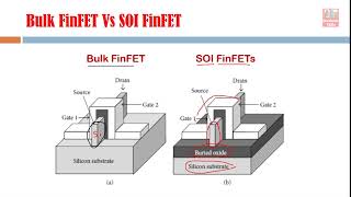
FinFET Structures
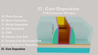
FinFET process flow
TSMC 5nm, 3nm and 2nm devices explained | Technology Node | VLSI | Why such naming? | TSMC
FinFETs
FinFET transistor
Latch Up in CMOS | SCR Latch Up Analogy | Latch up in CMOS Inverter | Latch up prevention in CMOS
Why FinFETs ? Part 1
Semitracks: Intel Ivy Bridge 22nm FinFET Process Fabrication
FinFET Design By Dr K G Sharma
FinFET technology | SG & IG | Part1 | VLSI | Lec-87
Channel Length Modulation in MOSFET (Basics, Physical Understanding, Derivation & Characteristics)
FPGA Architecture | Configurable Logic Block ( CLB ) | Part-1/2 | VLSI | Lec-75
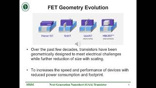
Next Generation Nanosheet GAA Transistor
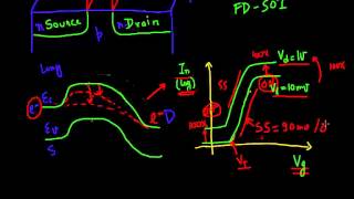
112N. Velocity saturated MOSFETs, short channel effects, SOI, FinFET, Pillar FET, Strained Silicon