Home
Discover: die-to-wafer hybrid bonding | CEA-Leti
CEA-Leti
Aug 22, 2023
32,379 views
How an ASML Lithography Machine Moves a Wafer
Discover: hybrid bonding | CEA-Leti
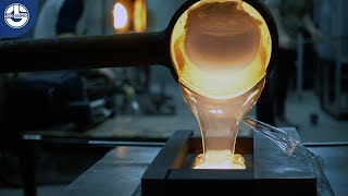
How Glass is Made | From Mining Silica to Wonders of Glass!
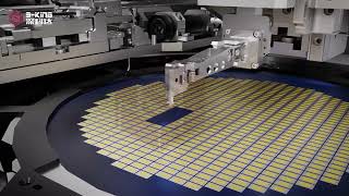
S-King Product: Flip Chip Die Bonder (High Precision Solution)
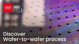
Discover: wafer-to-wafer hybrid bonding | CEA-Leti
Wafer-Bond-Anlage und -Verfahren
Why Wafer Bonding is the Future of Semiconductors
Stacking Dies For Performance and Profit
The process of making seals whose prints float and disappear! Amazing factory in Japan!
Semiconductor Packaging - ASSEMBLY PROCESS FLOW
Besi 8800 automated by i-Operator # CASTEC
How are BILLIONS of MICROCHIPS made from SAND? | How are SILICON WAFERS made?
Packaging Part 12 - Hybrid Bonding 1
LBSemicon 공정소개영상(한국어)_엘비세미콘
1 Packaging Process Technology TSMC and Intel, CoWoS, EMIB, Foveros and Chiplets
MICRONAS - Micronas Backend Overview
Walking Through a Big PCB Factory in China | JLCPCB
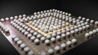
The World of Advanced Packaging
IEDM: Enabling Hybrid Bonding on Intel Process
Inside Micron Taiwan’s Semiconductor Factory | Taiwan’s Mega Factories EP1