Home
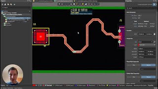
3 Basic Tricks For EMC Compliant PCB Layout
Sentineo Embedded Electronics
17 ก.พ. 2023
การดู 7,357 ครั้ง
Altium Designer RF Impedance Matching (e.g. 50Ω, USB, ...)
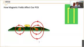
How GND VIAs Improve Your PCB Layout
High Speed PCB Design: How-To? Mastering The Basics For Success
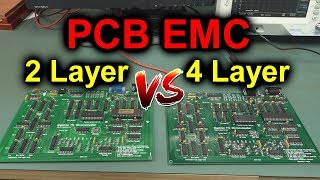
EEVblog #1176 - 2 Layer vs 4 Layer PCB EMC TESTED!
RF Engineering | Skillsets for Modern RF Engineers
How To Design a Rigid Flex PCB in Altium Designer
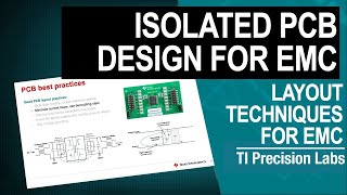
Optimizing isolated PCB design for EMC
I2C and SPI on a PCB Explained!
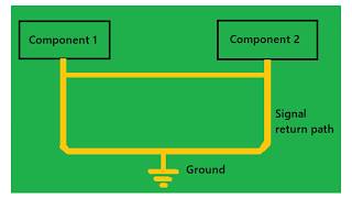
PCB Layout Fundamentals
Two-Layer PCB Design Tips: Achieving the Optimal Layout
6 Horribly Common PCB Design Mistakes
Super Quick Component Placement in Altium Designer #pcbdesignfreesoftware #altium #altiumdesigner
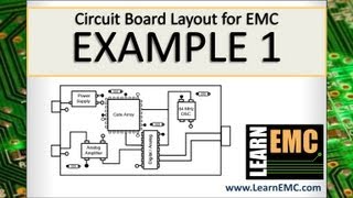
Circuit Board Layout for EMC: Example 1
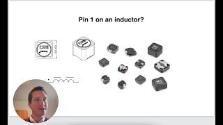
Why Does An Inductor Have A Pin 1?
PCB Design for EMI & SI - Phil's Lab #64
EMI/EMC Part 1: Intro to EMI/EMC Simulation
Why is 50 OHM impedance used in PCB Layout? | Explained | Eric Bogatin | #HighlightsRF
How To Do High-Speed Length Tuning in Altium Designer
Schematic Tips & Tricks - Phil's Lab #62
PCB Design for minimising Electromagnetic interference